
Blog

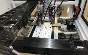
In the world of Contract Electronic Manufacturing, recent advances in technology have allowed companies to gain significant efficiencies. It is possible to reduce manufacturing costs considerably by increasing throughput. Today’s equipment enables contract manufacturers (CMs) to achieve greater speed with higher first pass yields. The speed and accuracy of the latest machinery is often the most significant differentiator among CMs.

What are the most important things to consider when searching for an electronics manufacturer? The best partnerships strike a fine balance between specialized knowledge, capacity, capabilities, quality, dependability, flexibility & pricing. Most companies do their best to vet potential contract manufacturers and quite often the responsibility for research and data collection is given to a junior team member.


As I began writing, the article I started to write felt entirely self-serving. I was just sharing a personal experience. An experience that impacted my thinking and further raised my respect for the organization I joined last year, but unfortunately, the article failed to meet the criteria I have recommended over the years. The advice I typically give is; make sure you share something that may be useful or helpful to the readers.

The implementation of a new growth strategy in 2017 produced pleasing results for our company. We are eagerly kicking off the new year by increasing our production capabilities to meet the growing demand. The first week of 2018 was marked by the arrival of new equipment and it is now up and running!

A few weeks ago, I had the pleasure of sitting down and speaking with a couple of gentlemen who collectively had more than 60 years’ experience in a global industry. In the early years of their business, they were able to use domestic suppliers for everything, but as competition in their space grew, prices were driven down, and they like many other original equipment manufacturers, found it necessary to source product components overseas.

Electronic Manufacturing Service (EMS) providers are often asked to do the impossible. In most cases “the impossible” refers to the delivery deadline. Industry veterans know what it takes to produce their products, and they consider the timeline challenges of their EMS when planning product launches and production runs. Those who do not, often find themselves wrestling with supply chain and product delivery issues.

Outsourcing electronics manufacturing and assembly can provide a wide range of benefits to companies who choose wisely. Not every project is a good fit for all manufacturers, but having an electronics manufacturer who brings more to the table than merely executing the prescribed instructions on a PO, should pay significant dividends.
A few weeks ago, I shared an article that explained the basics of conformal coatings. The article provided a brief description of the benefits of coatings, with the most obvious benefit being, they create a barrier between sensitive surface mount device and the environment in which they function. I also mentioned some additional protections they provide, such as protecting solder contacts from thermal and mechanical shock, and corrosion.
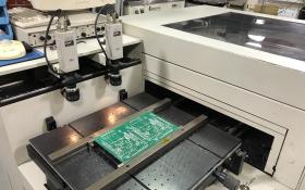
Solder paste is commonly used to create electrical connections and mechanical bonds between printed circuit board pads and surface mount devices, such as resistors and capacitors. It is made up of powdered solder in a flux paste. The flux serves several purposes. It removes oxidation from metallic surfaces, it protects the components to be soldered, as well as the metallic surface on the board.